Cooperation Agreement for
Small Form-Factor Pluggable Transceivers
Agilent
Technologies, Blaze Network Products, E2O Communications, Inc.,
ExceLight
Communications, Finisar Corporation, Fujikura Technology America Corp.,
Hitachi Cable,
Infineon Technologies Corp., IBM Corp., Lucent Technologies,
Molex, Inc.,
Optical Communication Products, Inc., Picolight, Inc.,
Stratos Lightwave, Tyco Electronics
I.
Purpose of the
Cooperation Agreement (Agreement)
Each party desires to establish internationally
compatible sources of a pluggable fiber optic transceiver module in support of
standards for fiber optic systems including Asynchronous Transfer Mode (ATM),
FDDI, Fibre Channel, Fast Ethernet and Gigabit Ethernet, and Synchronous
Optical Network (SONET) / Synchronous Digital Hierarchy (SDH) applications.
Each party further desires to establish uniformity
in the industry for the Transceiver “Package Dimensions”, “Cage and Electrical
Connector System”, “Host Board Layout”, “Electrical Interfaces”, and “Front
Panel Bezel Requirements” as described in Appendices A-B.
Each party expects that the establishment of compatible
sources for an interchangeable transceiver module will allow the entire fiber
optic marketplace to grow more rapidly.
This enhanced marketplace growth, customer choice, and vigorous
competition are the express purposes of this Agreement. Each
party acknowledges this agreement provides a solution with height as a primary
limiting constraint and may not provide an optimum solution for applications
with different constraints.
The parties desire to establish compatible sources
for additional products in the future.
II.
Agreement
A. General
The parties agree to
cooperate by supporting common product specifications for pluggable fiber optic
transceivers with the package “Package Dimensions”, “Cage and Electrical
Connector System”, “Host Board Layout”, “Electrical Interfaces”, and “Front
Panel Bezel Requirements” as shown in Appendices A-B. The overall package dimensions shall not exceed the maximum
indicated dimensions, and the mounting features shall be located such that the
products are mechanically interchangeable with the cage and connector
system. In addition the overall
dimensions and mounting requirements for the cage and connector system on a
circuit board shall be configured such that the products are mechanically and
electrically interchangeable.
The electrical and optical specifications shall be
compatible with those enumerated in the appropriate standards (i.e. the IEEE
802.3z Gigabit Ethernet standard and the ITU G.957 Synchronous Digital
Hierarchy standard). Recommended circuit layouts for electrical input and
output terminations, and grounding practices are also described in Appendix B.
The transceivers per this agreement will accept an optical connector such as the duplex
LC, MT-RJ or the SG connector. This agreement does not preclude any of the
parties from offering SFP transceivers with other connectors.
Internal design of the SFP transceiver is entirely
at the discretion of each party and is not covered by this Agreement. The parties recognize that their products
may not be identical, but need only meet the above criteria.
B.
Licensing and Fees
No license is granted under the patents, know-how,
tradesecrets or any other technology of any party to this Agreement either
expressly or by implication or by estoppel.
Each of the MSA parties have agreed that licenses to all required
intellectual property will be made available to all interested parties under reasonable
and non-discriminatory terms and conditions applicable to that MSA party. Individual parties to this Agreement may
have patents, which they believe may be relevant to this Agreement. The MSA parties should be contacted
individually to determine if they have patent rights, which they believe may be
pertinent to this Agreement. Each party
is free to seek technology or other exchanges with other firms in order to
support its activities under this Agreement.
C.
Scope of the Agreement
The scope of this Agreement
includes transceivers with transmission rates up to 5.0 Gb/s operating over
multimode and single mode fiber.
Each party agrees to be responsible for its own
development, manufacturing, marketing and selling in order to supply
transceivers meeting the attached specifications.
This Agreement does not preclude any party from
offering other products that may not meet the attached specifications.
Each party retains complete liberty regarding its
methods of implementing a supply of product, e.g., by engineering effort or by
technology licensing or transfer or combination of these or other practices.
Each party also retains sole discretion in its
choice of sales channels and distribution.
Each party affirms its intention to compete freely
and openly in the marketplace with the parties as well as other competitors.
Each party expects to support products meeting the
attached specifications for as long as marketplace conditions warrant. No specific time limit is associated with
this Agreement. The determination of
market condition suitability is to be made by each party individually and in
each party’s sole discretion.
III.
Public Announcement
A. Announcing the Agreement
Each party agrees to
announce this Agreement in a manner agreed upon by the parties. These announcements will mention all the
parties who have signed this Agreement.
Each party agrees to seek public attention by means
of such an announcement.
Each party agrees to
contribute time and effort at its sole discretion toward preparing and making
such an announcement.
B. Promotion of the Agreement
After the Agreement is
announced, each party may advertise or otherwise promote this Agreement in any
way that it deems appropriate. Mutual
consent of the other party is required if such other party is to be mentioned
by name.
IV.
Other Vendors
A. Other Vendors Matching the Product
Configuration
The parties recognize that additional vendors may
choose to match the attached product specifications after this Agreement is
announced.
Each party recognizes it is desirable and keeping
with the intent of the Agreement for such additional vendors to support the
transceiver mechanical dimensions and functional attributes described in
Appendix A.
Therefore, each party agrees
to encourage other vendors to support these product specifications.
B. Naming Other Vendors
Each party agrees to have written internal
procedures that require such party to name the other parties when customers ask
who intends to be a source for transceivers as described in this
Agreement. Each party agrees for such
procedures to require it to name the others regardless as to whether another of
the parties has already supplied similar transceiver products to that customer.
An example of suggested wording is: “Agilent, Blaze
Networks, E2O, ExceLight, Finisar, Fujikura, Hitachi Cable, Infineon, IBM,
Lucent, Molex, OCP, Picolight, Stratos Lightwave, and Tyco have signed a
Cooperation Agreement relating to the establishment of Small Form-factor
Pluggable transceivers for multimode and single mode fiber operating up to 5.0
Gb/s data rates.”
The parties are not obligated to provide any
information other than the identities of the other parties. The requirements of this provision are met
entirely if a party has the aforementioned written procedures and they are made
available to its sales force in the same way as are other sales related
procedures.
V.
Future Direction
A.
Current Product
Should the parties agree to further explore technical and other
exchanges pertaining to the products described in this Agreement, then this
shall be under a separate agreement.
B.
Withdrawal
The parties recognize that
at some future time it may become less feasible to offer the products
envisioned by this Agreement. A party
may withdraw from its commitment to cooperate at its own discretion upon a 90-day
notice to the other parties. This
notice is necessary to allow the other parties to discontinue mentioning the
withdrawing part as a participant in this Agreement and to reconsider any
jointly planned promotional activities.
VI.
Limitation of
Liability
With the exception of disputes arising out of
intellectual property issues, no party to
this Agreement shall be liable for any indirect, incidental, punitive, or
consequential damages, including without limitation, lost profits or changes of
good will, or similar losses, even if advised of the possibility of such
damages. In addition, each party’s
liability under this Agreement for direct damages shall be limited to $10,000.
Appendix A. Mechanical Interface
A1. SFP Transceiver Package
Dimensions
A2. Mating of SFP Transceiver PCB to
SFP Electrical Connector
A3. Host Board Layout
A4. Insertion, Extraction and
Retention Forces for SFP Transceivers
A5. Labeling of SFP Transceivers
A6. Bezel Design for Systems Using
SFP Transceivers
A7. SFP Electrical Connector
Mechanical Specifications
A8. SFP Cage Assembly Dimensions
Appendix B. Electrical
Interface
B1. Introduction
B2. Pin Definitions
B3. Timing Requirements of Control
and Status I/O
B4. Module Definition Interface and
Data Field Description
Appendix C. Agreement
Signatures
Appendix A.
Mechanical Interface
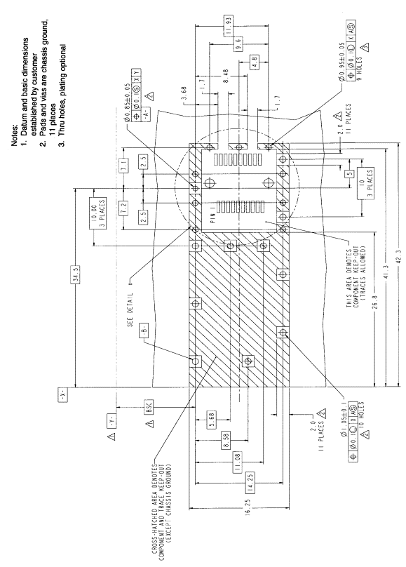
A1. SFP Transceiver Package Dimensions
A common mechanical outline
is used for all SFP transceivers. The
package dimensions for the SFP transceiver are described in Table 1 and Figures
1A and 1B.
Table 1. Dimension Table for Drawing of SFP
Transceiver
Designator
|
Dimension
(mm)
|
Tolerance
(mm)
|
Comments
|
|
A
|
13.7
|
± 0.1
|
Transceiver
width, nosepiece or front that extends inside cage
|
|
B
|
8.6
|
± 0.1
|
Transceiver
height, front, that extends inside cage
|
|
C
|
8.5
|
± 0.1
|
Transceiver
height, rear
|
|
D
|
13.4
|
± 0.1
|
Transceiver
width, rear
|
|
E
|
1.0
|
Maximum
|
Extension
of front sides outside of cage, see Note 2 Figure 1B
|
|
F
|
2.3
|
Reference
|
Location
of cage grounding springs from centerline, top
|
|
G
|
4.2
|
Reference
|
|
|
H
|
2.0
|
Maximum
|
Width
of cage grounding springs
|
|
J
|
28.5
|
Minimum
|
|
|
K
|
56.5
|
Reference
|
|
|
L
|
1.1x45°
|
Minimum
|
Chamfer
on bottom of housing
|
|
M
|
2.0
|
± 0.25
|
Height
of rear shoulder from transceiver printed circuit board
|
|
N
|
2.25
|
± 0.1
|
Location
of printed circuit board to bottom of transceiver
|
|
P
|
1.0
|
± 0.1
|
Thickness
of printed circuit board
|
|
Q
|
9.2
|
± 0.1
|
Width
of printed circuit board
|
|
R
|
0.7
|
Maximum
|
Width
of skirt in rear of transceiver
|
|
S
|
45.0
|
± 0.2
|
Length
from latch shoulder to rear of transceiver
|
|
T
|
34.6
|
± 0.3
|
Length
from latch shoulder to bottom opening of transceiver
|
|
U
|
41.8
|
± 0.15
|
Length
from latch shoulder to end of printed circuit board
|
|
V
|
2.5
|
± 0.05
|
Length
from latch shoulder to shoulder of transceiver outside of cage (location of
positive stop).
|
|
W
|
1.7
|
± 0.1
|
Clearance
for actuator tines
|
|
X
|
9.0
|
Reference
|
Transceiver
length extending outside of cage, see Note 2 Figure 1B
|
|
Y
|
2.0
|
Maximum
|
Maximum
length of top and bottom of transceiver extending outside of cage, see Note 2
Figure 1B
|
|
Z
|
0.45
|
± 0.05
|
Height
of latch boss
|
|
AA
|
8.6
|
Reference
|
Transceiver
height, front, that extends inside cage
|
|
AB
|
2.6
|
Maximum
|
Length
of latch boss (design optional)
|
|
AC
|
45°
|
± 3°
|
Entry
angle of actuator
|
|
AD
|
0.3
|
Maximum
|
Radius
on entry angle of actuator
|
|
AE
|
6.3
|
Reference
|
Width
of cavity that contains the actuator
|
|
AF
|
2.6
|
± 0.05
|
Width
of latch boss (design optional)
|
|
AG
|
0.40
|
Minimum
|
Maximum
radius of front of latch boss, 2 places (design optional)
|
Figure 1A. Drawing of SFP Transceiver
Figure 1B. Drawing
of SFP Transceiver (Cont.)
A2. Mating of SFP Transceiver PCB to SFP Electrical Connector
The SFP transceiver contains a
printed circuit board that mates with the SFP electrical connector. The pads
are designed for a sequenced mating:
·
First mate – ground
contacts
·
Second mate – power
contacts
·

 Third mate – signal contacts
The design of the mating
portion of the transceiver printed circuit board is illustrated in Figure 2 and
the electrical pad layout is illustrated in Figure 3. A typical contact pad
plating for the printed circuit board is 0.38 micrometers minimum hard gold
over 1.27 micrometers minimum thick nickel. Other plating options that meet the performance
requirements are acceptable.

Figure 2. Recommended Pattern Layout for SFP Printed Circuit Board
Figure 3. SFP Transceiver Electrical Pad Layout
A3. Host
Board Layout
A typical host board mechanical
layout for attaching the SFP Connector and Cage System is shown in Figures 4A
and 4B.
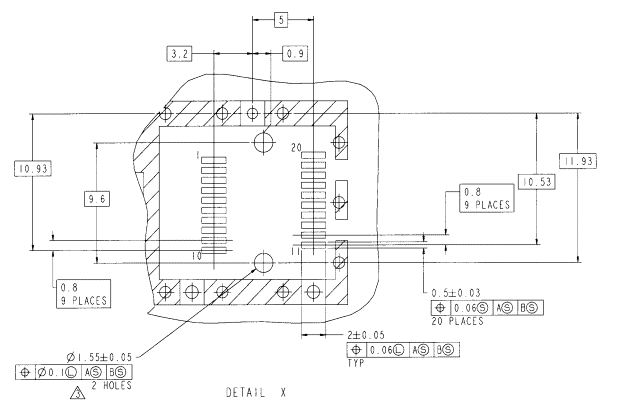
Figure
4B. SFP Host Board Mechanical Layout
(Cont.)
A4. Insertion, Extraction and Retention Forces
for SFP Transceivers
The requirement for the various functional forces and the
durability cycles are specified in Table 2.
Table 2. Insertion, Extraction, and Retention Forces
|
Measurement
|
Minimum
|
Maximum
|
Units
|
Comments
|
|
SFP transceiver insertion
|
0
|
40
|
Newtons
|
|
|
SFP transceiver extraction
|
0
|
11.5
|
Newtons
|
|
|
SFP transceiver retention
|
90
|
170
|
Newtons
|
No damage to
transceiver below 90N
|
|
Cage retention (Latch strength)
|
180
|
N/A
|
Newtons
|
No damage to
latch below 180N
|
|
Cage kickout spring force
|
11.5
|
22
|
Newtons
|
|
|
Insertion / removal cycles, connector/cage
|
100
|
N/A
|
cycles
|
|
|
Insertion / removal cycles, SFP transceiver
|
50
|
N/A
|
cycles
|
|
A5. Labeling
of SFP Transceivers
Color coding requirements for optical SFP
transceivers are specified in Figure 1B.
Each SFP transceiver should be clearly labeled. The
complete labeling need not be visible when the SFP transceiver is
installed. Labeling should include
appropriate manufacturing and part number identification, appropriate
regulatory compliance labeling, and a clear specification of the external port
characteristics. The external port
characteristic label may include such information as optical wavelength,
required fiber characteristics, operating data rate, interface standards
supported, and link length supported.
A6. Bezel Design for
Systems Using SFP Transceivers
Host enclosures that use SFP
devices should provide appropriate clearances between the SFP transceivers to
allow insertion and extraction without the use of special tools and a bezel
enclosure with sufficient mechanical strength. For most systems a nominal
centerline to centerline spacing of 16.25mm (0.640”) is sufficient. See Figure
5 for the recommended bezel design. For double-sided board mounting, a printed
circuit board thickness of 3.0mm (0.118”) is required.
The
SFP transceiver insertion slot should be clear of nearby moldings and covers
that might block convenient access to the latching mechanisms, the SFP
transceiver, or the cables connected to the SFP transceiver.
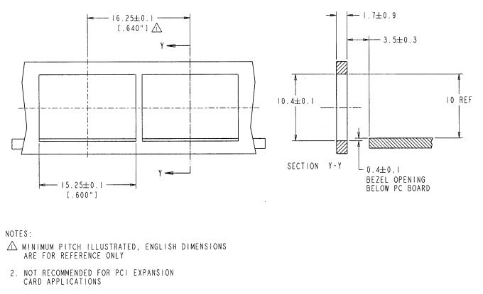
Figure 5. Recommended Bezel Design
A7. SFP Electrical Connector Mechanical
Specifications
The SFP Connector is a
20-contact, right angle surface mount connector. It is described in Table 3 and
Figure 6. The plating on the contacts is specified as follows:
·
Contact area: 0.38 micrometers minimum hard gold over 2.54 micrometers
minimum thick nickel
·
Solder terminal area:
gold flash or 2.54 micrometers tin lead plating over 2.54 minimum thick nickel.
Table 3. SFP Transceiver
Connector Dimensions
|
Designator
|
Dimension
(mm)
|
Tolerance
(mm)
|
Comments
|
|
A
|
9.4
|
± 0.08
|
Connector card slot
width
|
|
B
|
1.4
|
± 0.05
|
Guide pin diameter
|
|
C
|
11.2
|
Maximum
|
Connector width
|
|
D
|
9.2
|
Maximum
|
Connector length
|
|
E
|
3.5
|
Reference
|
Distance from
centerline of connector to outer contact
|
|
F
|
3.9
|
Reference
|
Distance from
centerline of connector to outer contact
|
|
G
|
1.35
|
Maximum
|
Connector card slot
height
|
|
H
|
2.6
|
Minimum
|
Height from bottom
of connector to bottom of card slot
|
|
J
|
9.6
|
TP
|
Distance between
guide pins
|
|
K
|
0.9
|
Reference
|
Diamond guide pin
width
|
|
L
|
1.4
|
± 0.05
|
Diamond guide pin
length
|
|
M
|
5.4
|
Maximum
|
Connector height
|
|
N
|
0.8
|
Reference
|
Length of solder
leads past housing, front & rear
|
|
P
|
6.0
|
Minimum
|
Depth of card slot
from front face of housing
|
|
Q
|
3.0
|
Maximum
|
Depth of contact
point from front face of connector
|
|
R
|
0.7
|
± 0.1
|
Size of chamfer on
top face of connector
|
|
S
|
0.3
|
Reference
|
Distance boss
extends past front face of connector
|
|
T
|
1.0
|
Minimum
|
Size of chamfer at
entry of card slot, all around
|
|
U
|
4.5
|
Reference
|
Length from
centerline of guide posts to end of solder lead
|
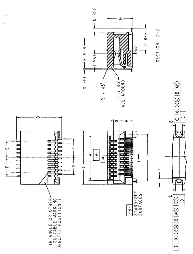
Figure 6. SFP Transceiver Connector Illustration
A8. SFP Cage Assembly Dimensions
The SFP Cage Assembly
consists of two components: a lower cage that is soldered to the host board and
a top cage that is assembled to the lower cage after soldering. A reference
drawing describing the SFP Cage Assembly is provided in Table 4 and Figures 7A
and 7B. The cage material is copper alloy and plating options are:
·
Tin-lead
plate 2.54 micrometers minimum over copper flash
·
Tin
plate 2.54 micrometers minimum over 0.76 micrometers minimum nickel
Table 4. Dimension Table for
Drawing of SFP Cage Assembly
|
Designator
|
Dimension
(mm)
|
Tolerance
(mm)
|
Comments
|
|
A
|
48.8
|
Maximum
|
Overall
length
|
|
B
|
8.3
|
Maximum
|
|
|
C
|
14.0
|
± 0.1
|
Inside
width of cage
|
|
D
|
14.25
|
Basic
|
Distance
between solderleg centerlines on side of cage
|
|
E
|
0.249
|
± 0.025
|
Thickness
of solderleg
|
|
F
|
9.0
|
Basic
|
Distance
between vent holes along length
|
|
G
|
11.8
|
Basic
|
Distance
from front of cage to beginning of center vent hole row
|
|
H
|
7.9
|
Basic
|
Distance
between vent holes across the width of the cage
|
|
J
|
2.0
|
± 0.1
|
Diameter
of vent holes
|
|
K
|
16.5
|
Basic
|
Distance
from front of cage to solderleg
|
|
L
|
10.0
|
Basic
|
Distance
between chassis ground solderlegs along side
|
|
M
|
0.6
|
± 0.1
|
Width
of EMI pins
|
|
N
|
0.7
|
± 0.1
|
Width
of all chassis ground solderlegs
|
|
P
|
2.0
|
Maximum
|
Width
of solderleg shoulder
|
|
Q
|
1.25
|
Maximum
|
Length
of solderleg
|
|
R
|
3.95
|
Basic
|
Distance
from centerline of cage to centerline of chassis ground solderleg
|
|
S
|
1.45
|
Basic
|
Distance
from centerline of cage to centerline of chassis ground solderleg
|
|
T
|
1.45
|
Basic
|
Distance
from centerline of cage to centerline of chassis ground solderleg
|
|
U
|
4.8
|
Basic
|
Distance
from centerline of cage to centerline of EMI pins
|
|
V
|
0.5
|
± 0.05
|
Width
of EMI pins on top cage
|
|
W
|
9.2
|
± 0.15
|
Distance
from inside top of cage to inside bottom surface of front section of cage
assembly
|
|
X
|
9.8
|
Maximum
|
Maximum
height of cage assembly from host board
|
|
Z
|
10.0
|
Basic
|
Distance
between chassis ground solderlegs along side
|
|
AA
|
11.5
|
Basic
|
Distance
from front of cage to solderleg
|
|
AB
|
7.5
|
Minimum
|
Length
of 9.2 (W) dimension from front of cage
|
|
AC
|
15.0
|
Maximum
|
Maximum
width of cage assembly
|
|
AD
|
13.9
|
Minimum
|
Minimum
width of inside of cage
|
|
AE
|
8.95
|
± 0.15
|
Height
of inside of cage assembly
|
|
AF
|
1.0
|
Minimum
|
|
|
AG
|
2.4
|
Basic
|
Distance
of clearance slots from cage centerline
|
Table 4. Dimension Table for Drawing of SFP Cage
Assembly (Cont.)
|
Designator
|
Dimension
(mm)
|
Tolerance
(mm)
|
Comments
|
|
AH
|
3.0
|
± 0.1
|
Width
of clearance slots
|
|
AJ
|
2.35
|
± 0.1
|
Distance
from front of cage to latch opening
|
|
AK
|
2.8
|
± 0.1
|
Length
of latch opening
|
|
AL
|
0.5
|
Minimum
|
Height
of latch lead-in
|
|
AM
|
45.6
|
Maximum
|
Distance
from front of cage to kickout spring
|
|
AN
|
35.0
|
Maximum
|
Distance
from front of cage to end of cage floor
|
|
AP
|
0.7
|
± 0.1
|
Width
of solderlegs that extend from floor of cage
|
|
AQ
|
5.1
|
Maximum
|
Width
of latch
|
|
AR
|
3.0
|
± 0.05
|
Width
of latch opening
|
|
AS
|
16.3
|
Basic
|
Front
of cage to beginning of outer vent hole rows
|
|
AT
|
0.65
|
Maximum
|
Inside
radius of cage, four places
|
|
AU
|
5.8
|
Minimum
|
Distance
between panel ground spring supports
|
|
AV
|
12.7
|
Maximum
recommended
|
Length
of plug extending outside of the cage
|
|
AW
|
15.75
|
Maximum
|
Width
of plug extending outside of the cage
|
|
AX
|
10.9
|
Maximum
|
Height
of plug extending outside of the cage
|
A9.
Dust / EMI Cover
The order to
prevent contamination of the internal components and to optimize EMI
performance, it is recommended that a Dust/EMI Plug be inserted into cage
assemblies when no transceiver is present.
The maximum dimensions of the Dust/EMI Cover are listed in Table 4 and
the maximum size is illustrated in Figure 7A.
The Dust/EMI Cover shall exert a maximum force of 4.0 Newtons per side
to the inside surfaces of the cage.
This force shall be measured as the force/side required to compress the
Dust/EMI Cover’s compliant feature(s) to the maximum dimensions listed in Table
4 (Illustrated in Figure 7A).
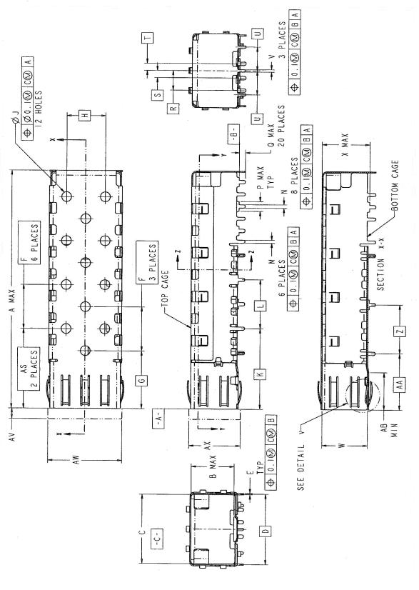
Figure 7A. SFP Cage Assembly
Figure
7B. SFP Cage Assembly (Cont.)
Appendix
B. Electrical Interface
B1.
Introduction
This annex contains pin definition data for the
small form-factor pluggable (SFP) transceiver. The pin definition data is
specific to gigabit rate datacom applications such as Fibre Channel and Gigabit
Ethernet. It is expected that different
pin definitions will be developed for SONET/ATM and lower data rate datacom
applications.
B2.
Pin Definitions
Figure
1 below shows the pin names and numbering for the connector block on the host
board. The diagram is in the same
relative orientation as the host board layout (see Appendix A, Figure 4.). As mentioned, this pinout only applies to
gigabit rate datacom applications. The
pin functions are defined in Table 1 and the accompanying notes. Figure 2A shows the recommended power supply
filtering network. Figure 2B shows an
example of a complete SFP host board schematic with connections to SerDes and
protocol ICs. For EMI protection the
signals to the 20-pin connector should be shut off when the transceiver is removed. Standard board layout practices such as
connections to Vcc and GND with Vias, use of short- and equal-length
differential signal lines, use of microstrip-lines and 50W terminations are recommended. Chassis grounds and external electromagnetic interference shields
should not be attached to circuit ground.
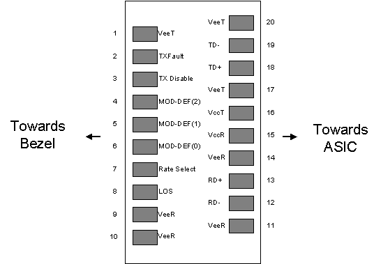
Figure 1.
Diagram of Host Board Connector Block Pin Numbers and Names
Table 1. Pin
Function Definitions
|
Pin Num.
|
Name
|
Function
|
Plug
Seq.
|
Notes
|
|
1
|
VeeT
|
Transmitter
Ground
|
1
|
|
|
2
|
TX Fault
|
Transmitter
Fault Indication
|
3
|
Note 1
|
|
3
|
TX Disable
|
Transmitter Disable
|
3
|
Note 2
Module disables on high or open
|
|
4
|
MOD-DEF2
|
Module
Definition 2
|
3
|
Note 3, 2 wire
serial ID interface
|
|
5
|
MOD-DEF1
|
Module Definition 1
|
3
|
Note 3, 2 wire
serial ID interface
|
|
6
|
MOD-DEF0
|
Module Definition 0
|
3
|
Note 3, Grounded in
Module
|
|
7
|
Rate Select
|
Select between
full or reduced
receiver bandwidth
|
3
|
Note 4
Low or Open – reduced bandwidth,
High– full bandwidth
|
|
8
|
LOS
|
Loss of Signal
|
3
|
Note 5
|
|
9
|
VeeR
|
Receiver Ground
|
1
|
Note 6
|
|
10
|
VeeR
|
Receiver Ground
|
1
|
Note 6
|
|
11
|
VeeR
|
Receiver Ground
|
1
|
Note 6
|
|
12
|
RD-
|
Inv. Received Data
Out
|
3
|
Note 7
|
|
13
|
RD+
|
Received Data Out
|
3
|
Note 7
|
|
14
|
VeeR
|
Receiver Ground
|
1
|
Note 6
|
|
15
|
VccR
|
Receiver Power
|
2
|
3.3 ± 5%, Note 8
|
|
16
|
VccT
|
Transmitter Power
|
2
|
3.3 ± 5%, Note 8
|
|
17
|
VeeT
|
Transmitter
Ground
|
1
|
Note 6
|
|
18
|
TD+
|
Transmit Data In
|
3
|
Note 9
|
|
19
|
TD-
|
Inv. Transmit Data
In
|
3
|
Note 9
|
|
20
|
VeeT
|
Transmitter
Ground
|
1
|
Note 6
|
Plug Seq.: Pin engagement sequence during hot plugging.
1) TX Fault is an open collector/drain output, which should be
pulled up with a 4.7K – 10KW resistor on
the host board. Pull up voltage between
2.0V and VccT, R+0.3V. When high,
output indicates a laser fault of some kind.
Low indicates normal operation. In the low state, the output will be
pulled to < 0.8V.
2)
TX disable is an
input that is used to shut down the transmitter optical output. It is pulled up within the module with a 4.7
– 10 KW
resistor. Its states are:
Low (0 –
0.8V): Transmitter on
(>0.8, < 2.0V): Undefined
High (2.0 – 3.465V): Transmitter
Disabled
Open: Transmitter
Disabled
Table 1 Notes (Cont.)
3)
Mod-Def 0,1,2. These are the module definition pins. They should be pulled up with a 4.7K – 10KW resistor on the host board. The pull-up voltage shall be
VccT or VccR (see Section IV for further details).
Mod-Def 0 is grounded by the module to indicate that the module is present
Mod-Def 1 is the clock line of two wire serial interface for serial ID
Mod-Def 2 is the data line of two wire serial interface for serial ID
4)
This is an optional
input used to control the receiver bandwidth for compatibility with multiple
data rates (most likely Fibre Channel 1x and 2x Rates). If implemented, the input will be internally
pulled down with > 30kW resistor. The
input states are:
Low (0 – 0.8V): Reduced
Bandwidth
(>0.8 , < 2.0V): Undefined
High (2.0 – 3.465V): Full Bandwidth
Open: Reduced
Bandwidth
5)
LOS (Loss of Signal)
is an open collector/drain output, which should be pulled up with a 4.7K – 10KW resistor. Pull up voltage between 2.0V and VccT,
R+0.3V. When high, this output
indicates the received optical power is below the worst-case receiver
sensitivity (as defined by the standard in use). Low indicates normal operation. In the low state, the output will
be pulled to < 0.8V.
6)
VeeR and VeeT may be
internally connected within the SFP module.
7)
RD-/+: These are the
differential receiver outputs. They are
AC coupled 100 W differential
lines which should be terminated with 100 W
(differential) at the user SERDES. The
AC coupling is done inside the module and is thus not required on the host
board. The voltage swing on these lines
will be between 370 and 2000 mV differential (185 – 1000 mV single ended) when
properly terminated.
8)
VccR and VccT are the
receiver and transmitter power supplies.
They are defined as 3.3V ±5% at the SFP connector pin. Maximum supply current is 300 mA. Recommended host board power supply filtering is shown below.
Inductors with DC resistance of less than 1W should
be used in order to maintain the required voltage at the SFP input pin with
3.3V supply voltage. When the
recommended supply filtering network is used, hot plugging of the SFP
transceiver module will result in an inrush current of no more than 30 mA
greater than the steady state value.
VccR and VccT may be internally connected within the SFP transceiver
module.
9)
TD-/+: These are the
differential transmitter inputs. They
are AC-coupled, differential lines with 100W
differential termination inside the module. The AC coupling is done inside the
module and is thus not required on the host board. The inputs will accept differential swings of 500 – 2400 mV (250
– 1200 mV single-ended), though it is recommended that values between 500 and
1200 mV differential (250 – 600 mV single-ended) be used for best EMI
performance.
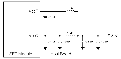
Figure 2A. Recommended Host Board Supply Filtering Network
Figure
2B. Example SFP Host Board Schematic
B3.
Timing Requirements
of Control and Status I/O
The timing requirements of the control and status lines are drawn largely from
the GBIC standard at the time of writing.
They are summarized in Table 2 below:
Table 2.
Timing Requirements of Control and Status I/0
|
Parameter
|
Symbol
|
Min
|
Max
|
Unit
|
Condition
|
|
TX
Disable Assert Time
|
t_off
|
|
10
|
ms
|
|
|
TX Disable Negate
Time
|
t_on
|
|
1
|
ms
|
|
|
Time to initialize,
including reset of TX_Fault
|
t_init
|
|
300
|
ms
|
From power on or
negation of TX Fault using TX Disable
|
|
TX Fault Assert
Time
|
t_fault
|
|
100
|
ms
|
Time from fault to
TX fault on.
|
|
TX Disable to reset
|
t_reset
|
10
|
|
ms
|
Time TX Disable
must be held high to reset TX_fault
|
|
LOS Assert Time
|
t_loss_on
|
|
100
|
ms
|
Time from LOS state
to RX LOS assert
|
|
LOS Deassert Time
|
t_loss_off
|
|
100
|
ms
|
Time from non-LOS
state to RX LOS deassert
|
|
Rate-Select Change
Time
|
t_ratesel
|
|
10
|
ms
|
Time from rising or
falling edge of Rate Select input until receiver bandwidth is in conformance
with appropriate specification.
|
|
Serial ID Clock
Rate
|
f_serial_clock
|
|
100
|
kHz
|
|
SFP
transceiver power on initialization procedure, TX_DISABLE negated.During power on of the SFP transceiver,
TX_FAULT, if implemented, may be asserted (High) as soon as power supply
voltages are within specification. For transceiver initialization with
TX_DISABLE negated, TX_FAULT shall be negated when the transmitter safety
circuitry, if implemented, has detected that the transmitter is operating in
its normal state. If a transmitter fault has not occurred, TX_FAULT shall be
negated within a period t_init from the time that VCCT exceeds the
specified minimum operating voltage (see Table 2). If TX_FAULT remains asserted
beyond the period t_init, the host may assume that a transmission fault has
been detected by the transceiver.
SFP
transceiver power on initialization procedure, TX_DISABLE negated (Cont.)
If no transmitter safety circuitry is
implemented, the TX_FAULT signal may be tied to its negated state.
The power-on initialization timing for
a transceiver with TX_DISABLE negated is shown in Figure 3.
Figure 3. Power on
initialization of SFP transceiver, TX_DISABLE negated
SFP transceiver power on initialization procedure, TX_DISABLE
asserted.
For SFP transceiver power on
initialization with TX_DISABLE asserted, the state of TX_FAULT is not defined
while TX_DISABLE is asserted. After TX_DISABLE is negated, TX_FAULT may be
asserted while safety circuit initialization is performed. TX_FAULT shall be
negated when the transmitter safety circuitry, if implemented, has detected
that the transmitter is operating in its normal state. If a transmitter fault
has not occurred, TX_FAULT shall be negated within a period t_init from the
time that TX_DISABLE is negated. If TX_FAULT remains asserted beyond the period
t_init, the host may assume that a transmission fault has been detected by the
transceiver.
If no transmitter safety circuitry is
implemented, the TX_FAULT signal may be tied to its negated state. The power-on initialization timing for a SFP
transceiver with TX_DISABLE asserted is shown in Figure 4.
Figure 4. Power on initialization of SFP, TX_DISABLE
asserted
Initialization
during hot plugging of SFP TRANSCEIVER.When a transceiver is not installed, TX_FAULT is held to the
asserted state by the pull up circuits on the host. As the SFP transceiver is
installed, contact is made with the ground, voltage, and signal contacts in the
specified order. After the SFP has determined that VCCT has reached
the specified value, the power on initialization takes place as described in
the above sections. An example of
initialization during hot plugging is provided in Figure 5.
Figure
5. Example
of initialization during hot plugging,
TX_DISABLE negated.
SFP
transmitter management
The timing requirements for the management of
optical outputs from the SFP transceiver using the TX_DISABLE signal are shown
in Figure 6. Note that the t on time
refers to the maximum delay until the modulated optical signal reaches 90% of
the final value, not just the average optical power.
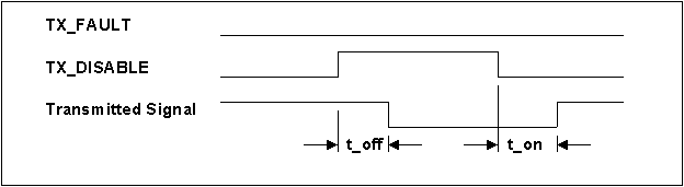 Figure 6.
SFP TX_DISABLE timing during normal operation.
Figure 6.
SFP TX_DISABLE timing during normal operation.
SFP transceiver fault detection and presentation
TX_FAULT shall be implemented by those
module definitions of SFP transceiver supporting safety circuitry. If TX_FAULT
is not implemented, the signal shall be held to the low state by the SFP
transceiver.
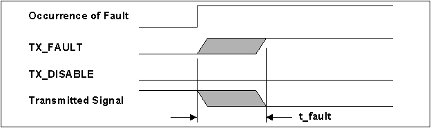
Figure 7. Detection
of transmitter safety fault condition
SFP transceiver fault recovery
The detection of a safety-related
transmitter fault condition presented by TX_FAULT shall be latched. The
following protocol may be used to reset the latch in case the transmitter fault
condition is transient. To reset the fault condition and associated detection
circuitry, TX_DISABLE shall be asserted for a minimum of t_reset. TX_DISABLE
shall then be negated. In less than the maximum value of t_init the optical
transmitter will correctly reinitialize the laser circuits, negate TX_FAULT,
and begin normal operation if the fault condition is no longer present. If a
fault condition is detected during the reinitialization, TX_FAULT shall again
be asserted, the fault condition again latched, and the optical transmitter
circuitry will again be disabled until the next time a reset protocol is
attempted. The manufacturer of the SFP shall ensure that the optical power
emitted from an open connector or fiber is compliant with IEC825-1 and CDRH
during all reset attempts, during normal operation or upon the occurrence
SFP transceiver fault
recovery (Cont.)
of
reasonable single fault conditions. The SFP transceiver may require internal
protective circuitry to prevent the frequent assertion of the TX_DISABLE signal
from generating frequent pulses of energy that violate the safety requirements.
The timing for successful recovery from a transient safety fault condition is
shown in Figure 8.
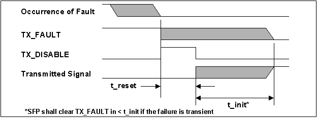
Figure 8. Successful
recovery from transient safety fault conditionAn example of an unsuccessful recovery, where the fault
condition was not transient, is shown in Figure 9.
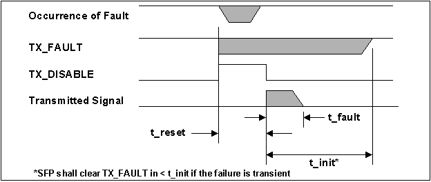
Figure 9. Unsuccessful recovery from safety fault
condition
SFP transceiver loss of signal indication
The LOS signal is intended as a
preliminary indication to the system in which the SFP transceiver is installed
that the link signals are likely to be outside the required values for proper
operation. Such indications typically point to non-installed cables, broken
cables, or a disabled, failing or powered off transmitter at the far end of the
cable. Additional indications are provided by the system in which the SFP
transceiver is installed to verify that the information being transmitted is
valid, correctly encoded, and in the correct format. Such additional
indications are outside the scope of the SFP TRANSCEIVER MSA.
The timing of the LOS function is specified in
Figure 10.

Figure 10.
Timing of LOS detection
B4.
Module Definition
Interface and Data Field Description
The definition of the MOD-DEF function is drawn largely from the GBIC standard
with some small, but backwards compatible, changes to the fields or allowed
values to reflect the latest standards and expectations for these
transceivers. In some cases, this
backward compatibility approach results in the possibility of illegal
combinations (such as defining an SFP module with SC optical connectors). Some locations previously reserved in the
GBIC serial identification have now been defined.
It
should be noted that only the serial module definition and the basic Mod-Def 0
indication of module present are implemented.
The use of MOD DEF lines as static codes for module definition as done
with GBIC are not implemented.
Overview
The SFP serial ID provides access to
sophisticated identification information that describes the transceiver’s
capabilities, standard interfaces, manufacturer, and other information. The
serial interface uses the 2-wire serial CMOS E2PROM protocol defined
for the ATMEL AT24C01A/02/04 family of components. When the serial protocol is activated, the host
generates the serial clock signal (SCL, Mod Def 1). The positive edge clocks data into those segments of the E2PROM
that are not write-protected within the SFP transceiver. The negative edge clocks data from the SFP
transceiver.The serial data signal (SDA, Mod Def 2) is
bi-directional for serial data transfer. The host uses SDA in conjunction with
SCL to mark the start and end of serial protocol activation. The memories are
organized as a series of 8-bit data words that can be addressed individually or
sequentially.
This section defines the information
structures that are obtained from the SFP transceiver via the serial ID.
A SFP transceiver shall meet the
electrical and optical requirements, including amplitude, eye diagram, jitter,
and other parameters, specified for the standards with which the transceiver
claims compliance.
Serial
information definition
The 2-wire serial CMOS E2PROM
provides sequential or random access to 8 bit parameters, addressed from 0000h
to the maximum address of the memory. The address select pins for the serial
CMOS E2PROM shall be set to zero (fixed at the VIL low
level). The fields specified by this section shall not be written by the host
in which it is installed. The SFP transceiver may enforce this by using the
write protect features of the CMOS E2PROM.
Serial information definition (Cont.)
The word address is transmitted with
the high order bit transmitted first. The protocol for the 2-wire serial
interface sequentially transmits one or more 8-bit bytes, with the data byte
addressed by the lowest word address transmitted first. In each data byte, the
high order bit (bit 7 in the accompanying tables) is transmitted first.
Numeric fields are expressed in binary,
with the high order byte being transferred first and the high order bit of each
byte being transferred first. Numeric fields are padded on the left with binary
zero values.
Character strings are ordered with the
first character to be displayed located in the lowest word address of the
string. Each character shall be coded as a US-ASCII character as defined by ISO
8859-1, with the high order bit transmitted first. All character strings will
be padded on the right with ASCII spaces (20h) to fill empty bytes.
All bits of reserved fields shall be
set to zero until future definitions require their use.
A minimum of 96 bytes shall be readable
by the serial identification process.
The maximum clock rate of the serial
interface shall be 100 KHz.
The following tables define the contents of the
serial CMOS E2PROM. The first table is a summary of all the data
fields in the serial ID chip. The remaining tables contain detailed
descriptions of the individual data fields.
Table
3.1. Serial ID: Data Fields
|
Data Address
|
Field Size
(Bytes)
|
Name of
field
|
Description
of field
|
|
|
BASE
ID FIELDS
|
|
0
|
1
|
Identifier
|
Type of
serial transceiver (see Table 3.2)
|
|
|
1
|
1
|
Ext.
Identifier
|
Extended
identifier of type of serial transceiver
|
|
|
2
|
1
|
Connector
|
Code for
connector type (see Table 3.3)
|
|
|
3-10
|
8
|
Transceiver
|
Code for
electronic compatibility or optical compatibility
(see Table
3.4)
|
|
|
11
|
1
|
Encoding
|
Code for
serial encoding algorithm (see Table 3.5)
|
|
|
12
|
1
|
BR, Nominal
|
Nominal bit
rate, units of 100 MBits/sec.
|
|
|
13
|
1
|
Reserved |
|
|
|
14
|
1
|
Length(9m) -
km
|
Link length
supported for 9/125 mm fiber, units of km
|
|
|
15
|
1
|
Length (9m)
|
Link length
supported for 9/125 mm fiber, units of 100 m
|
|
|
16
|
1
|
Length (50m)
|
Link length
supported for 50/125 mm fiber, units of 10 m
|
|
|
17
|
1
|
Length
(62.5m)
|
Link length
supported for 62.5/125 mm fiber, units of 10 m
|
|
|
18
|
1
|
Length
(Copper)
|
Link length
supported for copper, units of meters
|
|
|
19
|
1
|
Reserved
|
|
|
|
20-35
|
16
|
Vendor name
|
SFP
transceiver vendor name (ASCII)
|
|
|
36
|
1
|
Reserved
|
|
|
|
37-39
|
3
|
Vendor OUI
|
SFP
transceiver vendor IEEE company ID
|
|
|
40-55
|
16
|
Vendor PN
|
Part number
provided by SFP transceiver vendor (ASCII)
|
|
|
56-59
|
4
|
Vendor rev
|
Revision
level for part number provided by vendor (ASCII)
|
|
|
60-62
|
3
|
Reserved
|
|
|
|
63
|
1
|
CC_BASE
|
Check code
for Base ID Fields (addresses 0 to 62)
|
|
|
EXTENDED
ID FIELDS
|
|
|
64-65
|
2
|
Options
|
Indicates
which optional SFP signals are implemented
(see Table 3.6)
|
|
|
66
|
1
|
BR, max
|
Upper bit
rate margin, units of %
|
|
|
67
|
1
|
BR, min
|
Lower bit
rate margin, units of %
|
|
|
68-83
|
16
|
Vendor SN
|
Serial
number provided by vendor (ASCII)
|
|
|
84-91
|
8
|
Date code
|
Vendor’s
manufacturing date code (see Table 3.7)
|
|
|
92-94
|
3
|
Reserved
|
|
|
|
95
|
1
|
CC_EXT
|
Check code
for the Extended ID Fields (addresses 64 to 94)
|
|
|
VENDOR
SPECIFIC ID FIELDS
|
|
|
96-127
|
32
|
Read-only
|
Vendor
specific data, read only
|
|
|
128-511
|
384
|
Reserved
|
|
|
|
512-n
|
|
|
Vendor
specific
|
|
|
|
|
|
|
|
|
|
|
Identifier
The identifier
value specifies the physical device described by the serial information. This
value shall be included in the serial data. The defined identifier values are
shown in Table 3.2.
Table
3.2. Identifier Values
|
Value
|
Description
of Physical Device
|
|
00h
|
Unknown
or unspecified
|
|
01h
|
GBIC
|
|
02h
|
Module/connector
soldered to motherboard
|
|
03h
|
SFP
transceiver
|
|
04-7Fh
|
Reserved
|
|
80-FFh
|
Vendor
specific
|
Extended
Identifier
The field should be set to 04h for all
SFP modules indicating serial ID module definition.
ConnectorThe Connector value indicates the external
connector provided on the interface. This value shall be included in the serial
data. The defined connector values are shown in Table 3.3. Note that 01h – 05h
are not SFP compatible, and are included for compatibility with GBIC standards
TABLE 3.3. Connector Values
|
Value
|
Description
of Connector
|
|
00h
|
Unknown
or unspecified
|
|
01h
|
SC
|
|
02h
|
Fibre
Channel Style 1 copper connector
|
|
03h
|
Fibre
Channel Style 2 copper connector
|
|
04h
|
BNC/TNC
|
|
05h
|
Fibre
Channel coaxial headers
|
|
06h
|
FiberJack
|
|
07h
|
LC
|
|
08h
|
MT-RJ
|
|
09h
|
MU
|
|
0Ah
|
SG
|
|
0Bh
|
Optical
pigtail
|
|
0C-1Fh
|
Reserved
|
|
20h
|
HSSDC
II
|
|
21h
|
Copper
Pigtail
|
|
22h-7Fh
|
Reserved
|
|
80-FFh
|
Vendor
specific
|
Transceiver
The following
bit significant indicators define the electronic or optical
interfaces that are supported by the SFP transceiver. At least one bit shall be
set in this field. For Fibre Channel SFPs, the Fibre Channel speed,
transmission media, transmitter technology, and distance capability shall all
be indicated.
Table 3.4.
Transceiver codes
|
Data
Addr
|
Bit[1]
|
Description of transceiver
|
Data Addr
|
Bit1 |
Description of transceiver
|
|
Reserved Standard Compliance
Codes
|
Fibre Channel link length
|
|
3
|
7-0
|
Reserved
|
7
|
7
|
very long distance (V)
|
|
4
|
7-4
|
Reserved
|
7
|
6
|
short distance (S)
|
|
SONET Compliance Codes
|
7
|
5
|
intermediate distance (I)
|
|
4
|
3
|
Reserved
|
7
|
4
|
long distance (L)
|
|
4
|
2
|
OC 48, long reach
|
Fibre Channel transmitter
technology
|
|
4
|
1
|
OC 48, intermediate reach
|
7
|
3-2
|
Reserved
|
|
4
|
0
|
OC 48 short reach
|
7
|
1
|
Longwave laser (LC)
|
|
5
|
7
|
Reserved
|
7
|
0
|
Electrical inter-enclosure (EL)
|
|
5
|
6
|
OC 12, single mode long reach
|
8
|
7
|
Electrical intra-enclosure (EL)
|
|
5
|
5
|
OC 12, single mode inter. reach
|
8
|
6
|
Shortwave laser w/o OFC (SN)
|
|
5
|
4
|
OC 12 multi-mode short reach
|
8
|
5
|
Shortwave laser w/ OFC (SL)
|
|
5
|
3
|
Reserved
|
8
|
4
|
Longwave laser (LL)
|
|
5
|
2
|
OC 3, single mode long reach
|
8
|
0-3
|
Reserved
|
|
5
|
1
|
OC 3, single mode inter. reach
|
|
|
|
|
5
|
0
|
OC 3, multi-mode short reach
|
Fibre Channel transmission
media
|
|
|
|
|
9
|
7
|
Twin Axial Pair (TW)
|
|
|
|
|
9
|
6
|
Shielded Twisted Pair (TP)
|
|
|
|
|
9
|
5
|
Miniature Coax (MI)
|
|
Gigabit Ethernet Compliance Codes
|
9
|
4
|
Video Coax (TV)
|
|
6
|
7-4
|
Reserved
|
9
|
3
|
Multi-mode, 62.5m (M6)
|
|
6
|
3
|
1000BASE-T
|
9
|
2
|
Multi-mode, 50 m (M5)
|
|
6
|
2
|
1000BASE-CX
|
9
|
1
|
Reserved
|
|
6
|
1
|
1000BASE-LX
|
9
|
0
|
Single Mode (SM)
|
|
6
|
0
|
1000BASE-SX
|
|
|
|
|
|
|
|
Fibre Channel speed
|
|
|
|
|
10
|
7-5
|
Reserved
|
|
|
|
|
10
|
4
|
400 MBytes/Sec
|
|
|
|
|
10
|
3
|
Reserved
|
|
|
|
|
10
|
2
|
200 MBytes./Sec
|
|
|
|
|
10
|
1
|
Reserved
|
|
|
|
|
10
|
0
|
100 MBytes/Sec
|
Encoding
The encoding value indicates the serial encoding
mechanism that is the nominal design target of the particular SFP transceiver.
The value shall be contained in the serial data. The defined encoding values
are shown in Table 3.5.
Table 3.5. Encoding codes
|
code
|
Description of encoding
mechanism
|
|
00h
|
Unspecified
|
|
01h
|
8B10B
|
|
02h
|
4B5B
|
|
03h
|
NRZ
|
|
04h
|
Manchester
|
|
05h -FFh
|
Reserved
|
BR, nominal
The nominal
bit rate (BR, nominal) is specified in units of 100 Megabits per second,
rounded off to the nearest 100 Megabits per second. The bit rate includes those
bits necessary to encode and delimit the signal as well as those bits carrying
data information. A value of 0 indicates that the bit rate is not specified and
must be determined from the transceiver technology. The actual information
transfer rate will depend on the encoding of the data, as defined by the
encoding value.
Length (9m)-km
Addition to
EEPROM data from original GBIC definition. This value specifies the link length
that is supported by the SFP transceiver while operating in compliance with the
applicable standards using single mode fiber. The value is in units of
kilometers. A value of 255 means that the transceiver supports a link length
greater than 254 km. A value of zero means that the transceiver does not
support single mode fiber or that the length information must be determined
from the transceiver technology.
Length (9m)
This value
specifies the link length that is supported by the SFP transceiver while
operating in compliance with the applicable standards using single mode fiber.
The value is in units of 100 meters. A value of 255 means that the transceiver
supports a link length greater than 25.4 km. A value of zero means that the SFP
transceiver does not support single mode fiber or that the length information
must be determined from the transceiver technology.
Length (50m)
This value
specifies the link length that is supported by the SFP transceiver while
operating in compliance with the applicable standards using 50 micron
multi-mode fiber. The value is in units of 10 meters. A value of 255 means that
the SFP transceiver supports a link length greater than 2.54 km. A value of
zero means that the transceiver does not support 50 micron multi-mode fiber or
that the length information must be determined from the transceiver technology.
Length (62.5m)
This value
specifies the link length that is supported by the SFP transceiver while operating
in compliance with the applicable standards using 62.5 micron multi-mode fiber.
The value is in units of 10 meters. A value of 255 means that the SFP
transceiver supports a link length greater than 2.54 km. A value of zero means
that the SFP transceiver does not 62.5 micron multi-mode fiber or that the
length information must determined from the transceiver technology. It is
common for the SFP transceiver to support both 50 micron and 62.5 micron fiber.
Length (Copper)
This value
specifies the minimum link length that is supported by the SFP transceiver
while operating in compliance with the applicable standards using copper cable.
The value is in units of 1 meter. A value of 255 means that the SFP transceiver
supports a link length greater than 254 meters. A value of zero means that the
SFP transceiver does not support copper cables or that the length information
must be determined from the transceiver technology. Further information about
the cable design, equalization, and connectors is usually required to guarantee
meeting a particular length requirement.
Vendor name
The vendor
name is a 16 character field that contains ASCII characters, left-aligned and
padded on the right with ASCII spaces (20h). The vendor name shall be the full
name of the corporation, a commonly accepted abbreviation of the name of the
corporation, the SCSI company code for the corporation, or the stock exchange
code for the corporation. At least one of the vendor name or the vendor OUI
fields shall contain valid serial data.
Vendor OUI
The vendor
organizationally unique identifier field (vendor OUI) is a 3-byte field that
contains the IEEE Company Identifier for the vendor. A value of all zero in the
3-byte field indicates that the Vendor OUI is unspecified.
Vendor PN
The vendor
part number (vendor PN) is a 16-byte field that contains ASCII characters,
left-aligned and padded on the right with ASCII spaces (20h), defining the
vendor part number or product name. A value of all zero in the 16-byte field
indicates that the vendor PN is unspecified.
Vendor Rev
The vendor
revision number (vendor rev) is a 4-byte field that contains ASCII characters,
left-aligned and padded on the right with ASCII spaces (20h), defining the
vendor’s product revision number. A value of all zero in the 4-byte field
indicates that the vendor Rev is unspecified.
CC_BASE
The check code
is a one byte code that can be used to verify that the first 64 bytes of serial
information in the SFP transceiver is valid. The check code shall be the low
order 8 bits of the sum of the contents of all the bytes from byte 0 to byte
62, inclusive.
Options
The bits in the option field shall specify the
options implemented in the SFP transceiver as described in Table 3.6.
Table 3.6. Option Values
|
data
address
|
bit
|
Description of option
|
|
64
|
7-0
|
Reserved
|
|
65
|
7-6
|
Reserved
|
|
65
|
5
|
RATE_SELECT
is implemented
If
bit is set then active control of the rate select pin is required to change
rates. If bit is not set, no control
of pin is required. In all cases,
compliance with multiple rate standards should be determined by Transceiver
Codes in Bytes 4, 5, 6 and 10. (See
Table 3.4)
|
|
65
|
4
|
TX_DISABLE
is implemented and disables the serial output.
|
|
65
|
3
|
TX_FAULT
signal implemented. (Reset defined in section III)
|
|
65
|
2
|
Loss
of Signal implemented, signal inverted from definition in Table 1
NOTE:
This is not standard SFP transceiver behavior and should be avoided, since
non-interoperable behavior results.
|
|
65
|
1
|
Loss
of Signal implemented, signal as defined in Table 1
|
|
65
|
0
|
Reserved
|
BR, max
The upper bit
rate limit at which the SFP transceiver will still meet its specifications (BR,
max) is specified in units of 1% above the nominal bit rate. A value of zero
indicates that this field is not specified.
BR, min
The lower bit
rate limit at which the SFP transceiver will still meet its specifications (BR,
min) is specified in units of 1% below the nominal bit rate. A value of zero
indicates that this field is not specified.
Vendor
SN
The vendor
serial number (vendor SN) is a 16 character field that contains ASCII
characters, left-aligned and padded on the right with ASCII spaces (20h),
defining the vendor’s serial number for the SFP transceiver. A value of all
zero in the 16-byte field indicates that the vendor SN is unspecified.
Date
Code
The date code is an 8-byte field that contains
the vendor’s date code in ASCII characters. The date code is mandatory. The
date code shall be in the format specified by Table 3.7.
Table
3.7. Date Code
|
Data Address
|
Description of field
|
|
84-85
|
ASCII code,
two low order digits of year. (00 = 2000).
|
|
86-87
|
ASCII code,
digits of month (01 = Jan through 12 = Dec)
|
|
88-89
|
ASCII code,
day of month (01 - 31)
|
|
90-91
|
ASCII code,
vendor specific lot code, may be blank
|
CC_EXT
The check code is a one byte code that
can be used to verify that the first 32 bytes of extended serial information in
the SFP transceiver is valid. The check code shall be the low order 8 bits of
the sum of the contents of all the bytes from byte 64 to byte 94, inclusive.
Read-only
This area may
contain vendor specific information which can be read from the SFP transceiver.
The data is read only.
Appendix
C. Agreement Signatures
A. For
Agilent Technologies by:

_________________________________
Signed
Shane
Gibeson_____________________
Name
Business
Unit Manager_______________
Title
_________________________________
Date
B. For
Blaze Network Products by:
 _________________________________
Signed
Kirk
Bovill_________________________
Name
Director
of Product Marketing__________
Title
_________________________________
Date
C. For
E2O Communications, Inc. by:

_________________________________
Signed
H.
C. Lee__________________________
Name
President
and CEO__________________
Title
_________________________________
Date
D. For ExceLight
Communications, Inc. by:

_________________________________
Signed
Ed
Miskovic _______________________
Name
Director
of Marketing________________
Title
_________________________________
Date
E. For Finisar Corporation by:

_________________________________
Signed
Jerry
S. Rawls_____________________
Name
President
and Chief Executive Officer___
Title
_________________________________
Date
F.
For Fujikura
Technology America Corp. by:

_________________________________
Signed
Hirokazu
Hashimoto_________________
Name
President_________________________
Title
_________________________________
Date
G.
For Hitachi Cable
by:

_________________________________
Signed
Lou
Marra_________________________
Name
Engineering
Manager________________
Title
_________________________________
Date
H. For Infineon Technologies Corporation by:
 _________________________________
Signed
Schelto
Van Doorn__________________
Name
Engineering
Manager – Fiber Optics____
Title
_________________________________
Date
I. For
IBM Corporation by:

_________________________________
Signed
Dale
Crist_________________________
Name
Business
Line Manager, Transport______
Title
_________________________________
Date
J. For
Lucent Technologies by:

_________________________________
Signed
Margaret
Acker_____________________
Name
Marketing
Director___________________
Title
_________________________________
Date
K. For
Molex, Inc. by:

_________________________________
Signed
Tony
Dorin________________________
Name
Director
of Marketing________________
Title
_________________________________
Date
L. For
Optical Communication Products, Inc. by:

_________________________________
Signed
Mohammad
Ghorbanali______________
Name
Vice
President and COO_____________
Title
_________________________________
Date
M. For
Picolight, Inc. by:
 _________________________________
Signed
Chris
J. Simoneaux__________________
Name
Product
Line Manager________________
Title
_________________________________
Date
N. For
Stratos Lightwave by:

_________________________________
Signed
Jeff
Vetter_________________________
Name
Director
of Sales & Marketing__________
Title
_________________________________
Date
O. For
Tyco Electronics by:
 _________________________________
Signed
Glenn
Moore_______________________
Name
Vice
President_____________________
Title
_________________________________
Date